Chapter 3 - Carriers in Semiconductor
Pt. 1
ECE 4339
Han Q. Le
(copyrighted) U. of Houston
Part 1
0. Physical constants or frequently used formulas
1. Review classical conductivity: Drude model
1.1 Concept discussion
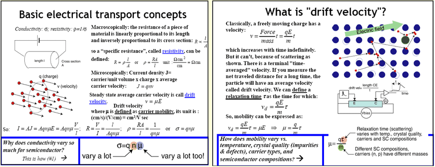
App Demo: Drude model of electron transport 1
App Demo: Concept of mobility
Look up the number of outer shell electrons
(conduction electrons) per atom of Au, Cu, Al, Ni. Look up their
specic density in gram/![]() .
Calculate the conduction electron density (# electrons per unit
volume, use unit
.
Calculate the conduction electron density (# electrons per unit
volume, use unit ![]() )
of these metals. From the looked up values of their
conductivities, calculate the electron drift velocity in these
metals.
)
of these metals. From the looked up values of their
conductivities, calculate the electron drift velocity in these
metals.
The electron mass in these metals is practically the same as free electron mass. Calculate their relaxation time.
1.2 Link to File on conductivity
2. Hall Effect
2.1 Basic discussion
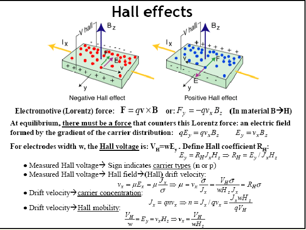
Consider a copper stripe with width w=0.5 cm. A current of 0.5 Ampere passes along its length. Plot the Hall voltage across its width as a function of magnetic induction field (use unit Gauss)
Extra reading on Hall effect:
As a young American student in 1879, Edwin H. Hall
discovered an unexpected phenomenon. He found that if a thin gold
plate is placed in a magnetic field at right angles to its surface
an electric current flowing along the plate can cause a potential
drop at right angles both to the current and the magnetic field.
Termed the Hall effect, this takes place because electrically
charged particles (in this case electrons) moving in a magnetic
field are influenced by a force and deflect laterally. The Hall
effect can be used to determine the density of charge carriers
(negative electrons or positive holes) in conductors and
semiconductors, and has become a standard tool in physics
laboratories the world over. Edwin Hall later joined Harvard
Physics Department in 1881 as a faculty. More than a century
later, Hall effect made science news again with the discovery of
Quantum Hall effect (or Quantized Hall effect), in which the Hall
resistance is quantized in unit and fraction of ![]() (Resistance=Volt/Amp=Volt
sec/charge=Volt charge sec/
(Resistance=Volt/Amp=Volt
sec/charge=Volt charge sec/![]() = Energy sec/
= Energy sec/![]() =
=![]() ).
The effect happens in two-dimensional electron gas in a
semiconductor quantum well. Shortly thereafter, fractional Quantum
Hall effects were also discovered. The discovers of the QHE were
awarded with the Nobel prizes.
).
The effect happens in two-dimensional electron gas in a
semiconductor quantum well. Shortly thereafter, fractional Quantum
Hall effects were also discovered. The discovers of the QHE were
awarded with the Nobel prizes.
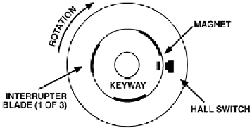
Hall-effect has been used to make sensors for engine, motor,
robotics, etc. As example, many of today's computerized engine
control systems are using Hall-Effect sensors, also called
Hall-Effect switches, to sense crankshaft and camshaft speed and
position. These switches vary in design but are similar in
operation. The main differences lie in the voltages at which they
work, physical configuration and location on the
engine. The Hall-Effect sensor is a very accurate way
for a computer to "see" the exact position or measure the speed of
a spinning shaft. Most designs utilize a shutter which passes
through an opening in the sensor. The opening has a magnetic field
passing across from a permanent magnet to the electronic switch.
When the shutter passes through the magnetic field, it
is interrupted and a change in voltage is sensed by the computer.
With the shutter in the opening, the voltage falls to near zero.
With the shutter out of the opening, the voltage rises to the
specified voltage level. This voltage is usually equal to battery
voltage on GM, Ford and many Chrysler engines. However, on
Chrysler 3.3L, 3.8L and 3.5L engines, the EC sends out an 8 volt
power supply and receives a 5 volt-0 volt signal back on the
sensor output wire. Some Hall Sensors use a moving magnet attached
to a timing chain sprocket (GM) or notches in the flex plate
(Chrysler) to generate a signal.
A charge moving in a magnetic field experiences an
electromotive force:
F=q v�B
in the y
direction: ![]()
(see drawing in the slide note the convention of the flow
direction)
Then there should be a current due to this force:
![]()
But where does this current go? It can�t just flow forever,
because the carrier will form a gradient with counter the follow
to reach a steady state. At equilibrium, there is no net flow and there must be a force that counters
this electromotive force. This force is an electric field
formed by the gradient of the carrier uneven distribution:
![]() or
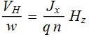
or ![]()
If the test electrodes are far apart by a width w, then the Hall
voltage is:
![]() .
.
When Hall first discovered the effect, he was using Au. The
carrier are electrons which have negative charge, and the Hall
voltage is negative. Years later, when people used the techniques
to study the transport properties of various materials, they
discovered that some materials have positive Hall effects. These
materials are semiconductors, and so they are called n-type (n for
negative) for negative Hall effect or p-type (p for positive) for
positive Hall effects. So this led to a puzzle in semiconductor
technology: what some have negative charge carrier and some have
positive charge carrier for the same semiconductor compound, e. g.
Ge. People knew that have something to do with impurities, but why
some are n and some are p?
Now a day, people do Hall measurement routinely to characterize a
material and they made various pattern to test.
Bonus homework: look up a commercial semiconductor Hall sensor (hint: GaAs). Get the spec sheet. Describe how it works and can be used to sense the magnetic marker for rotation speed sensing.
2.2 Hall effect conceptual illustration
2.2.1 Lorentz force - Classical motion
App Demo: Lorentz force - Hall effect - Demo 1
2.2.2 Hall voltage
App Demo: Hall Effect - Hall Voltage
2.3 Obtaining sample intrinsic properties
2.3.1 Drift velocity
At equilibrium, Hall voltage force must counter
balance Lorentz force:
![]() or
or
![]()
Let w be the strip
width, then:
![]()
Thus, we can
determine the drift velocity:

2.3.3 Carrier type and carrier density
Experimentally:
![]()
which can be understood with:
![]() and
and  (the
Drude model of conductivity)
(the
Drude model of conductivity)
In fact, substitute:
Or: 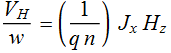
we obtain the quantity:
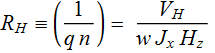
denoted as the Hall coefficient
![]() ,
which is the inverse of the conducting carrier charge density, an
intrinsic property of the sample.
,
which is the inverse of the conducting carrier charge density, an
intrinsic property of the sample.
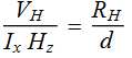
When we do measurements:
![]() ,
,
a positive or
negative ![]() will tell
immediately whether we have p-type or n-type carriers
will tell
immediately whether we have p-type or n-type carriers
and the bulk
carrier density is:

Hence, the objective of the Hall measurement is to obtain the Hall coefficient.
2.3.5 2D carrier density or sheet carrier density.
Note this: 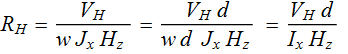
We measure ![]() and control
and control ![]() ,
,
![]() ,
hence, only the depth (or
thickness) of the conducting layer is needed to determine the
Hall coefficient. However, if we don�t know the depth,
then the measurement is simply for 2 D, i. e. all quantities are
related to areal rather than bulk. For example, since we don�t
know d, we just obtain the quantity:
,
hence, only the depth (or
thickness) of the conducting layer is needed to determine the
Hall coefficient. However, if we don�t know the depth,
then the measurement is simply for 2 D, i. e. all quantities are
related to areal rather than bulk. For example, since we don�t
know d, we just obtain the quantity:
Then: 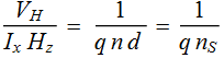
where ![]() is the 2D carrier density: carrier density per unit area, also
called the sheet density.
is the 2D carrier density: carrier density per unit area, also
called the sheet density.
2.3.2 Hall mobility
Recalling
that: σ=q n μ
We can obtain the mobility:
![]()
Hence, knowing the sample conductivity (by measuring its
resistance), the
Hall coefficient gives us the mobility.
2.4 Hall effect measurement simulation
http://www.nist.gov/pml/div683/hall_resistivity.cfm
2.4.1 Simulation
App Demo: Hall effect simulation
2.4.2 Additional note about unit
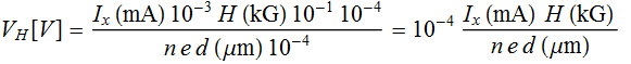
Be careful with unit when doing calculation. See below.
| Quantity | Standard Unit | Practical unit | Comment |
| A | mA or μA | Prefer current source | |
| V | V | Only if voltage source is used | |
| V | mV or μV | □ | |
| Sample thickness d | cm | μm | □ |
| Strip width w | cm | mm | Not relevant - for calc only |
| Strip length l | cm | mm | Not relevant -for calc only with V source |
| Carrier density n or p | □ | ||
| Mobility |
![]()
![]()
Note about Tesla: there is a factor ![]() to keep it consistent with all other quantities. For example about
Hall coeff
to keep it consistent with all other quantities. For example about
Hall coeff ![]()

We have to convert Tesla: 
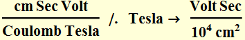
![]()
Hence, we must multiply ![]() to the numerical value of Hall coefficient
to the numerical value of Hall coefficient  to
have it in the unit of
to
have it in the unit of ![]() ,
,
Similarly, let�s consider 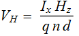

![]()
The output Hall voltage must be multiplied by ![]() to be in Volt. Suppose with use other units for other quantities,
we must include the conversion factor. Example:
to be in Volt. Suppose with use other units for other quantities,
we must include the conversion factor. Example:
Or: 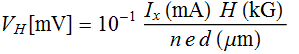
2.4.3 Simple calculator
App Demo: Hall effect simple calculator
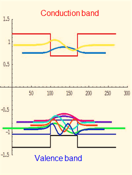
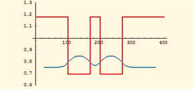
3. Band formation illustration
3.1 Concept introduction
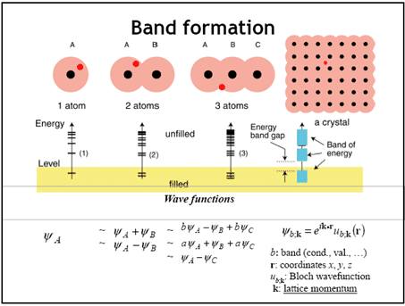
Example: one unit cell (example based on GaAs/AlGaAs quantum well with width=70 A).
This is just one state in level 2 (we call it conduction band)
Including many states for both levels 1 and 2. We will call level 1 valence band.
Example: two unit cells
We see that the wavefunction takes a shape that is a hybrid fusion of 2 basis wavefunctions of each QW.
There is an �antisymmetric� state that is not shown.
Example: three unit cells
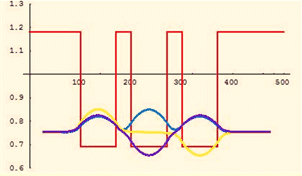
Example: six unit cells
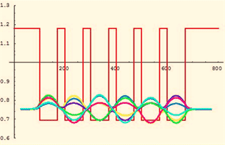
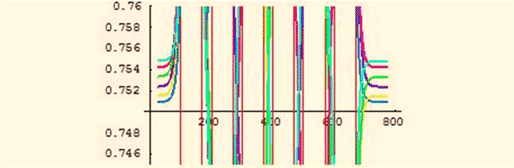
Note how closely the energy levels are by zooming
in:
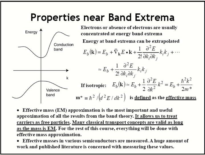
3.2 Bands and bandgap: concept introduction
The above is only for a hypothetical linear crystal with only 6 unit cells. We see that there are 6 energy levels between the range from 0.7505 to 0.7550 eV. Since each state above can actually accept 2 electrons of different spin (spin +1/2 and -1/2), there are 12 states for electrons to occupy.
But in a very large crystal with ![]() cells for example, the energy levels can be so densed together
that we can treat it conveniently as �continuous� within a range,
which we call a band.
cells for example, the energy levels can be so densed together
that we can treat it conveniently as �continuous� within a range,
which we call a band.
It is like having trillions and trillions of levels within 0.75 and 0.755 eV in the example above that we consider the range from 0.75 and 0.755 eV as a band, and energy is �practically continuous� within that band.
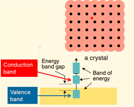
But the energy can still be quantized between different bands.
The energy gap between 2
bands is call a bandgap.
In
semiconductors, only 2 bands are important:
- an upper band that is mostly empty of electrons in a pure
crystal at absolute zero temperature, which we call �conduction band�;
- and the lower band beneath the conduction band that are
completely filled with electrons in a pure crystal at absolute
zero temperature, which we call �valence band.� (electrons in
valence band are what cause the bonding between atoms).
- The energy difference between
these two bands are called band gap energy or just �band gap�.
3.3 Density-of-state function: concept introduction
One important concept is based on the question: for a given system, how many states are available for electrons to occupy as a function of energy?
Digression: concept analogy: How many apartments are available for occupancy at a certain height level?


In the example of GaAs quantum wells with 6 unit cells, we know the answer is that there are 12 states between 0.7505 and 0.7550 eV.
But when the energy levels are so densed that
energy is practically continuous within a band, we use the concept
of density of state (DoS)
function: It is the number of states per unit of energy
at energy level E:
D(E)
ΔE = # states between E and E+ΔE
However, in the examples in 3.1, we see that with 3 unit cells, we have 3 states x 2 pins= 6 states. With 6 unit cells, we have 12 states. What if we have N unit cells? As we can guess, the answer is 2N states. Thus, the number of states is proportional to the number of atoms or molecules of a piece of semiconductor.
Hence, the appropriate concept for DoS is the number of states per unit of
energy (at energy level E) per unit volume.
D(E)
ΔE = # states between E and E+ΔE per unit volumn
4. Bloch wave function concept
4.1 Illustration
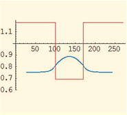
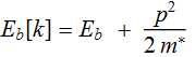
Below is a hypothetical Bloch wavefunction.
![]()
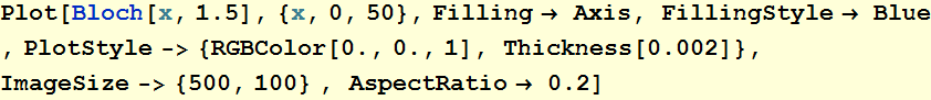
App Demo: Bloch wave function concept
The above illustrate two electrons with different momenta. Which one runs faster? and which one has longer wavelength. What is the relation of wavelength and speed?
4.2 Key concepts:
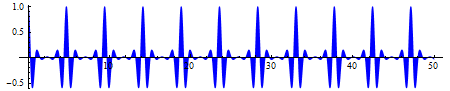
Momentum of such a wave is: ![]()
This value of momentum is what we use to obtain the effective
electron speed:
![]()
where ![]() is just some quantity that is a property of the system.
is just some quantity that is a property of the system.
It is obvious that ![]() has to be the mass of the electron. But note that we do not use
symbol m for the
electron mass, but
has to be the mass of the electron. But note that we do not use
symbol m for the
electron mass, but ![]() ,
because it is NOT electron mass. This will be the topic for the
next sub-section.
,
because it is NOT electron mass. This will be the topic for the
next sub-section.
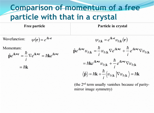
Interestingly, the energy associated with such wave
is:
where ![]() is some value that we call �band extremum energy� (or band edge
energy sometimes).
is some value that we call �band extremum energy� (or band edge
energy sometimes).
This looks just like classical result! but in reality, it is based on quantum mechanics. It just happens that the approximation for E[k] is classical-like, which makes it easy to comprehend.
4.3 Effective mass
Now we deal with the meaning of quantity ![]() above.
above.
Example
Below is a band in some semiconductor. The vertical
axis unit is eV. The horizontal axis unit is ![]() .
The shape of the band can be obtained by experimental measurements
or by theoretical calculation (very computing-intensive and
extensive).
.
The shape of the band can be obtained by experimental measurements
or by theoretical calculation (very computing-intensive and
extensive).
![]()
![]()
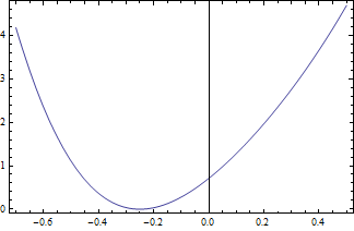
Find the effective mass
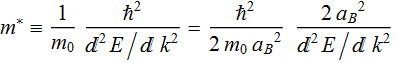
The effective mass is defined as:
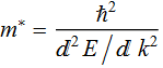
Usually, it is measured relative to the electron rest mass:
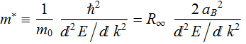
Assume the band energy is
![]()
![]()
![]()
![]()
![]()
![]()
![]()
![]()
The effective mass is (from the above):
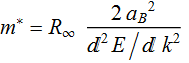
So we need to use appropriate energy unit for conversion.
![]()
![]()
![]()
![]()
![]()
![]()
The effective mass is 0.15 (relative to electron rest mass).
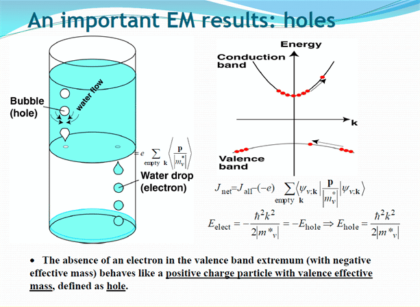
5. The absence of electron (electron void) in valence band: holes